
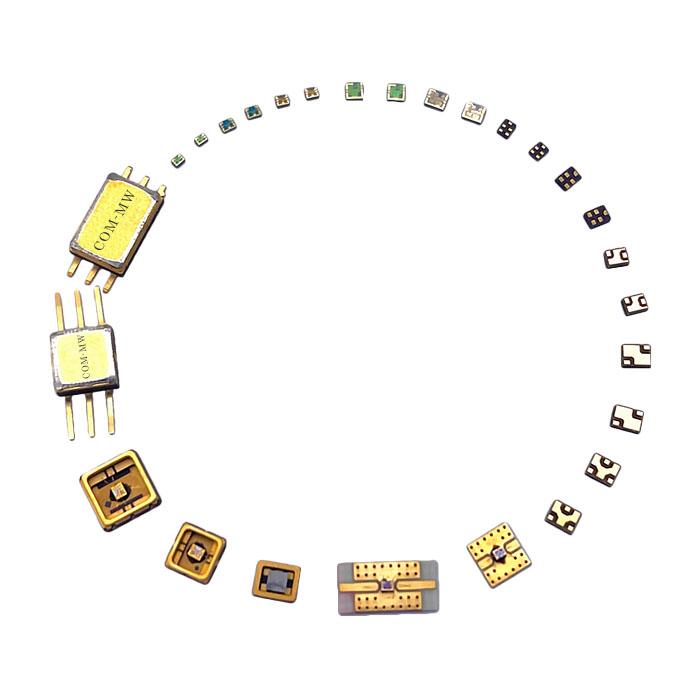
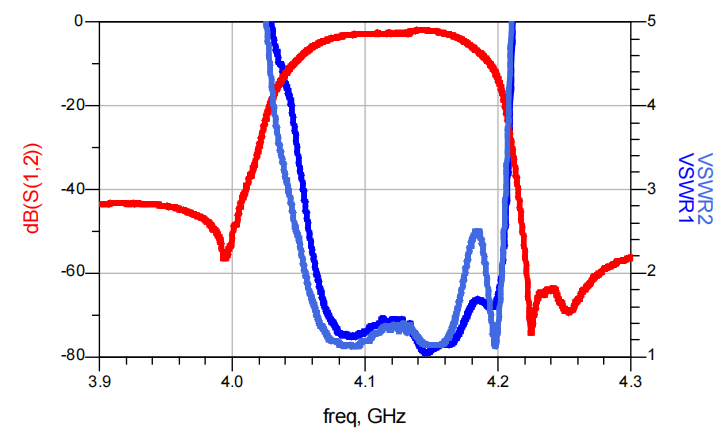
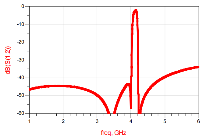
Passband4100MHz, 2GHz≥3840dB, 6GHz≥2830dB, Microstrip pad, FBAR
To check stock availability, search under "In-stock Products" on the Dianzibuy store.
Any change to the content of this page is subject to change without notice. Please confirm the specifications before ordering.
Products must not be used for any unlawful purpose; the customer bears any loss arising from unlawful use.
High precision FBAR process,
Small size, high performance, but sensitive to static electricity.
| Parameters | Frequency | / | Min | Typical | Max | Units |
|---|---|---|---|---|---|---|
| Passband | / | / | 4100 | MHz | ||
| Center loss | / | / | 3.0 | 3.5 | dB | |
| -1.0dB BW | / | / | point frequency | MHz | ||
| Rejection | 2 | GHz≥ | 38 | 40 | dB | |
| Rejection | 6 | GHz≥ | 28 | 30 | dB | |
| Passband VSWR | / | / | 1.8 | 2.0 |
| Connector | Microstrip pad |
| Impedance | 50Ω |
| Operation Temp. | -55~+85℃ Design assurance |
| Storage Temp. | -55~+125℃ Design assurance |
| Quality Grade | Industrial grade |
| ROHS | Compliant Available |
| Filter Category | FBAR |
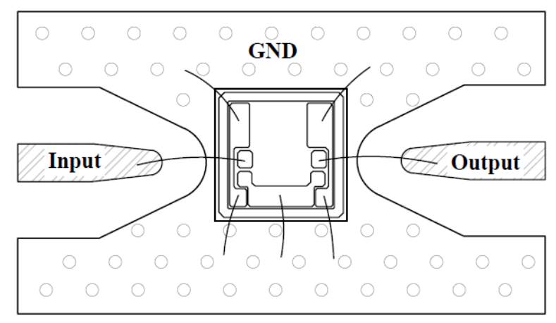
1. The chip needs to be sealed and stored in a nitrogen cabinet. After opening, please use it within 3 days. The chip needs to be assembled and used in a purified environment, and the chip ports are interchangeable,
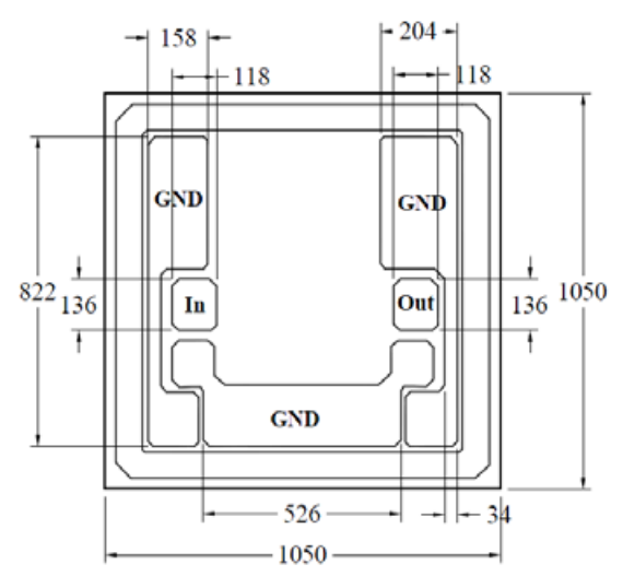
2. The chip needs to be clamped on both sides with precision pointed tweezers to avoid touching the surface of the chip. It is recommended to use low stress adhesive (preferably ME8456-DA) to bond the bottom of the chip, with an appropriate amount of adhesive to avoid excessive contamination of the front graphics,
3. After the chip is bonded, it can be cleaned using a plasma cleaning machine to avoid ultrasonic cleaning and liquid cleaning,
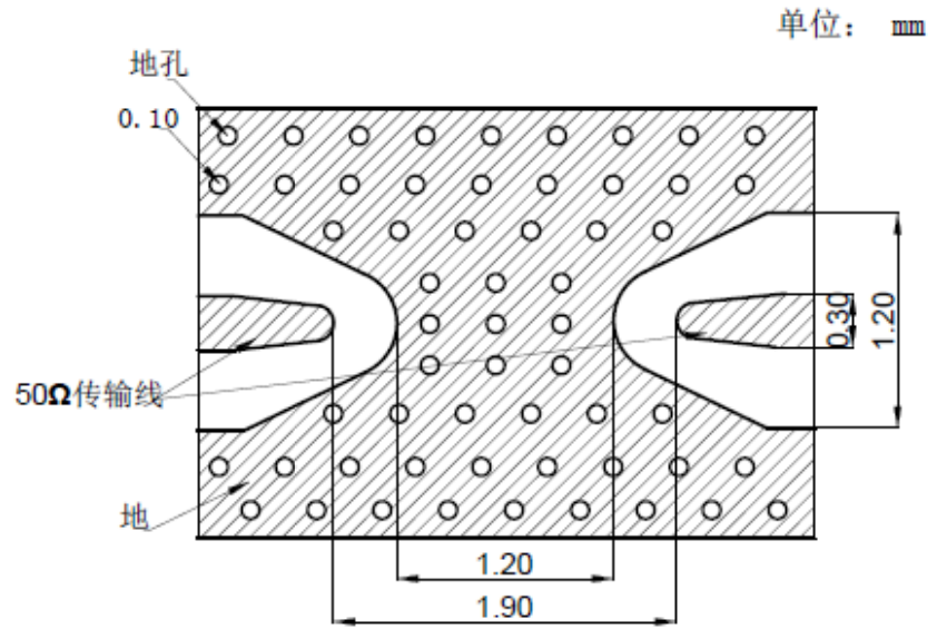
4. The performance of chips is affected by packaging form, wire specifications, length, and position. Please refer to the assembly diagram and consult the supplier. It is recommended to use wire bonding with a diameter of 25um.
Send us your requirements — our engineers will respond within one working day.