
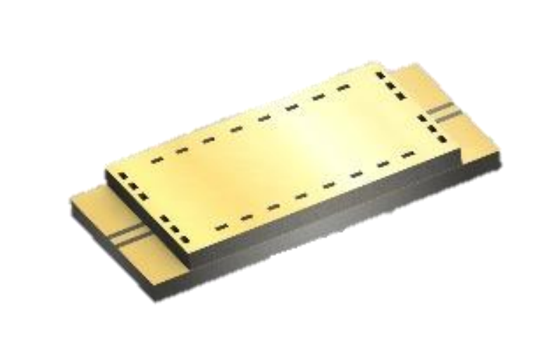
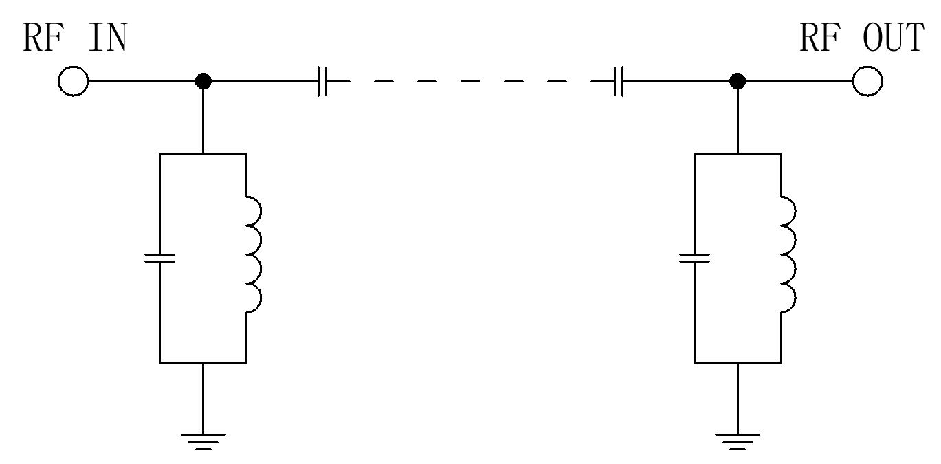
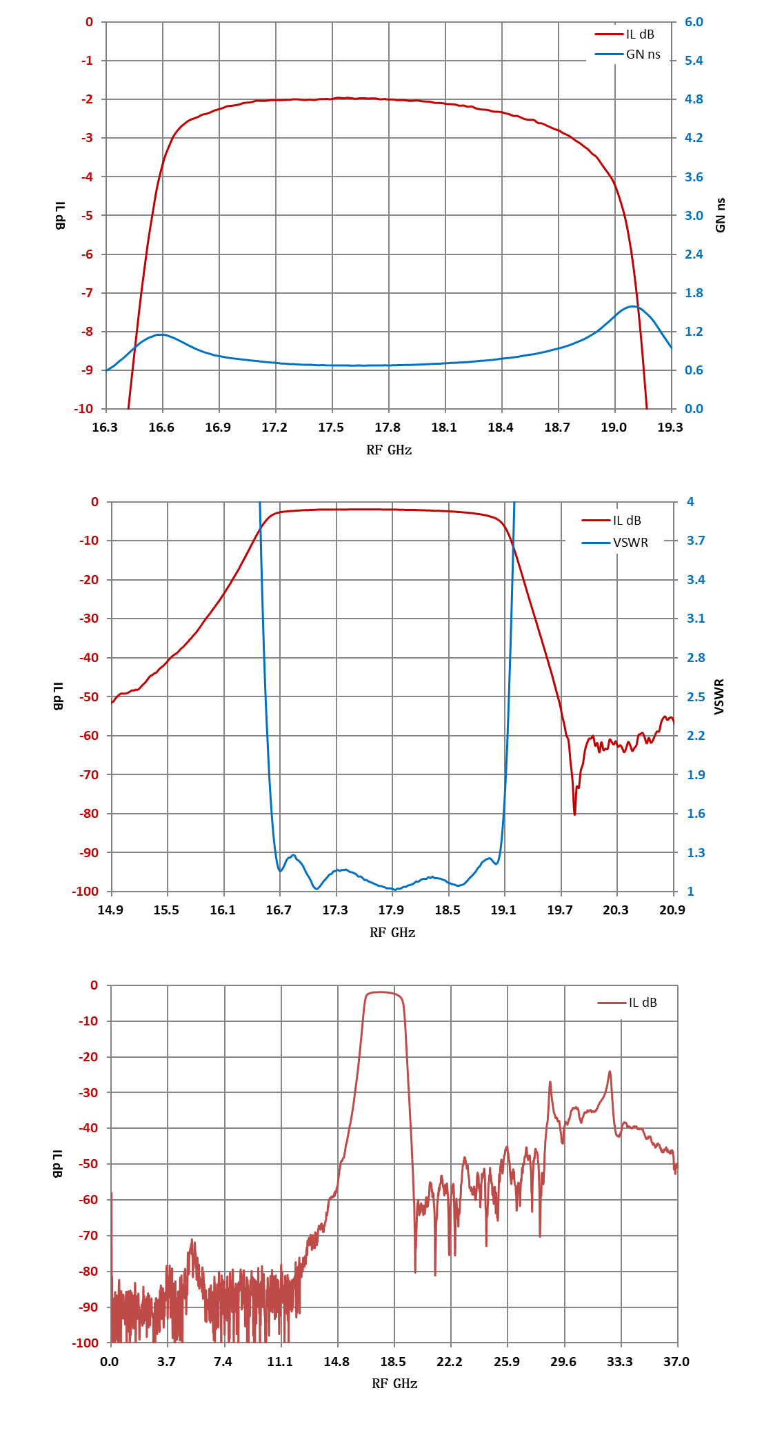
Bandwidth16.9-18.5GHz, Rejection40@DC-15.2GHz, 40@19.8-26.0GHz,
To check stock availability, search under "In-stock Products" on the Dianzibuy store.
Any change to the content of this page is subject to change without notice. Please confirm the specifications before ordering.
Products must not be used for any unlawful purpose; the customer bears any loss arising from unlawful use.
High precision MEMS process preparation
High performance, low-temperature float, small size.
Ceramic substrate, 50 Ω coplanar waveguide
Gold wire bonding
| Items | Parameters | Units |
|---|---|---|
| Center Frequency | 17.7 | GHz |
| Bandwidth | 16.9-18.5 | GHz |
| Center loss | 2.4 | dB |
| Ripple | 1.0 | dB |
| VSWR | 1.6:1 | |
| Group delay ripple | 0.5 | ns |
| Rejection | 40@DC-15.2GHz | dBc |
| Rejection | 40@19.8-26.0GHz | dBc |
| power | |
| Operation Temp. | -55~+85℃ |
| Storage Temp. | -55~+125℃ |
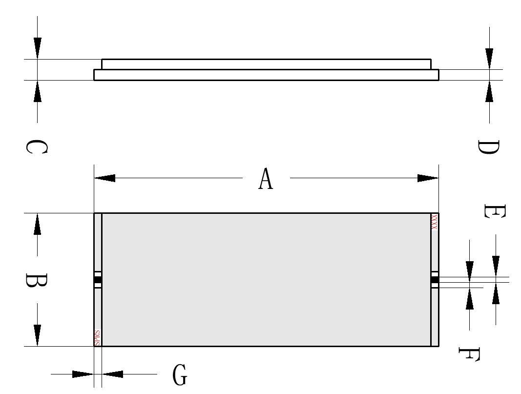
| Outline size | A:6.9,B:2.5,C:0.8,D:0.4,E:0.2,F:0.14,G:0.64 |
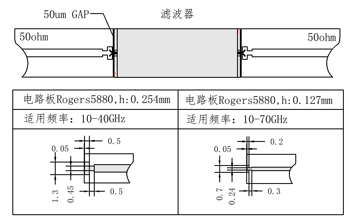
1: The chip is recommended to be used in separate chambers, with one side 0.1mm away from the side wall and the surface 2.2mm away from the top cover. The ports are interchangeable;
2: It is recommended to use low stress conductive adhesive (such as ME8456) to bond the chip, and connect it with no less than 2 25-50um gold wire bonding wires. The connecting wires should be as short as possible and the bonding height should be as low as possible;
3: The chip should be installed on Kovar (recommended) or a material with a thermal expansion coefficient similar to that of ceramics (6.7ppm/C), with a carrier thickness of ≥ 0.2mm, and cannot be directly soldered onto aluminum or copper shells;
4: Suggest using a T-shaped structure for microstrip bonding.
Send us your requirements — our engineers will respond within one working day.